 研究室の技術小史 ― 江刺研究室から田中(秀)研究室へ Brief technological history of MEMS Laboratory
仙台MEMSショールームのホームページも御覧下さい。 Please also visit Sendai MEMS showroom website.
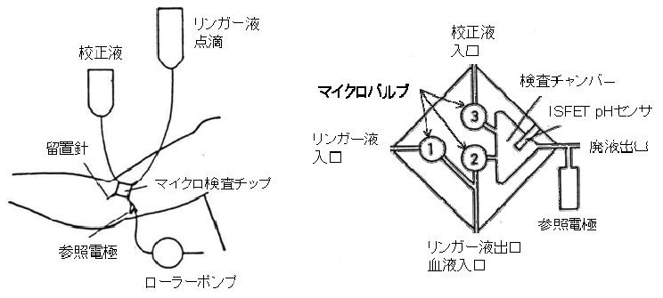 |
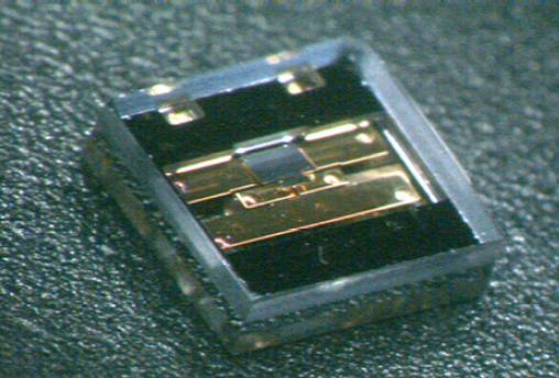
ISFETとマイクロバルブを集積化した血液検査チップ Integrated blood test chip with ISFET and microvalves
松尾教授(江刺教授の先生)と江刺教授が開発したISFET(Ion-Sensitive Field Effect Transistor)は,pHセンサなどとして様々なところで用いられています。クラレと新電元工業は,江刺教授らの研究成果をもとに血管内pH/pCO2モニタ用ISFETセンサを実用化しましたが,血管内でセンサの校正ができないという問題がありました。上図はその問題を解決す・驍スめに開発された血液検査チップであり,ISFET,マイクロバルブ,およびマイク・漉ャ路が集積化されています。昨今,このようなバイオ・医療マイクロデバイスの研究は広がりを見せており,実用化が期待されています。Prof. Matsuo (Supervisor of Prof. Esashi) and Prof. Esashi developed an ISFET (Ion-Sensitive Field Effect Transistor), which is widely used as pH sensors etc. Based on Prof. Esashi's research, a pH/pCO2 monitoring ISFET sensor used in blood vessels was commercialized by Kuraray and Shindengen Electric Manufacturing, but there was a problem that the calibration is impossible in a blood vessel. A blood test chip shown in the above figure, where the ISFET, microvalves and microchannels were integrated, was developed to solve this problem. Recently, research related this kind of biomedical microdevice is collecting a lot of attentions.
 |
 |
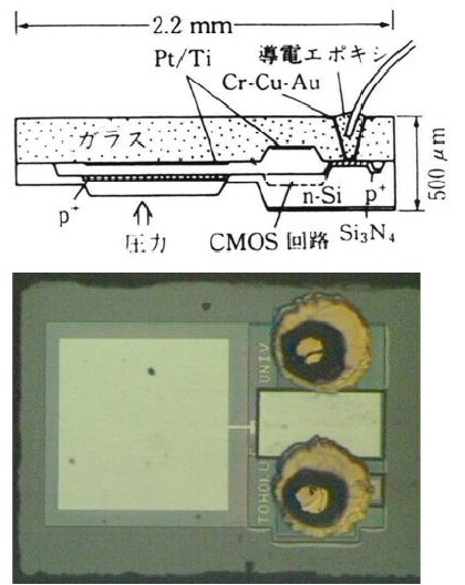
集積化静電容量型圧力センサ |
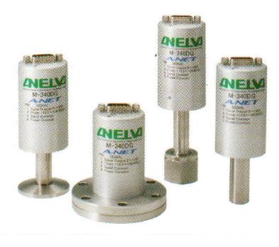
静電容量型真空圧力センサ(キャノンアネルバ) |
静電容量型圧力センサ Capacitive pressure sensor
静電容量型圧力センサは,圧力によるダイヤフラムの変形を,ダイヤフラムとそれに対向する電極との間の静電容量の変化として検出します。江刺教授らは,集積回路との一体化技術や真空封止された圧力基準空間からの電気配線取り出し技術を工夫し,上図の静電容量型集積化圧力センサを豊田工機(現JTEKT)と共同で実用化しました。また,キャノンアネルバと共同で静電容量型真空圧力センサも実用化しました。A capacitive pressure sensor measures the pressure-induced deformation of a diaphragm as a change of capacitance between the diapgragm and a counter electrode. Prof. Esashi developed and commercialized an integrated capacitive pressure sensor with Toyoda Machine Works (JTEKT at present). Our key technologies such as monolithic integration with a readout circuit and the wafer-level hermetic sealing of a pressure reference cavity are used. Prof. Esashi also developed and commercialized a capacitive vacuum pressure sensor with Canon Anelva.
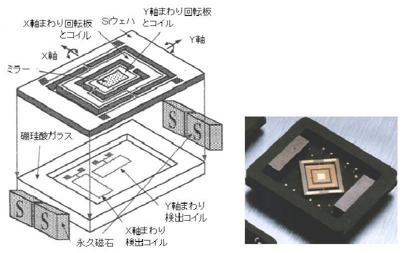 |
電磁駆動2軸光スキャナ Electromagnetically-driven 2-axis optical scanner
MEMS光スキャナの用途には,ヘッドアップディスプレイ,網膜ディスプレイ,携帯型レーザープロジェクタ,共焦点顕微鏡,カテーテル先でのOCT(Optical Coherence Tomography)システムなどがあります。上図は日本信号と共同開発された電磁駆動光スキャナであり,鉄道のホームドアの障害物検知システム,距離画像取得装置などで実用化されています。The applications of MEMS-based optical scanners include head-up display, retina display, mobile laser projector, confocal microscope and OCT (Optical Coherence Tomography) system for catheters. The above figure shows an electromagnetically-driven 2-axis optical scanner developed with Nippon Signal. This is commercially used in a safety detector of platform doors at railway stations, a time-of-flight range sensor etc.
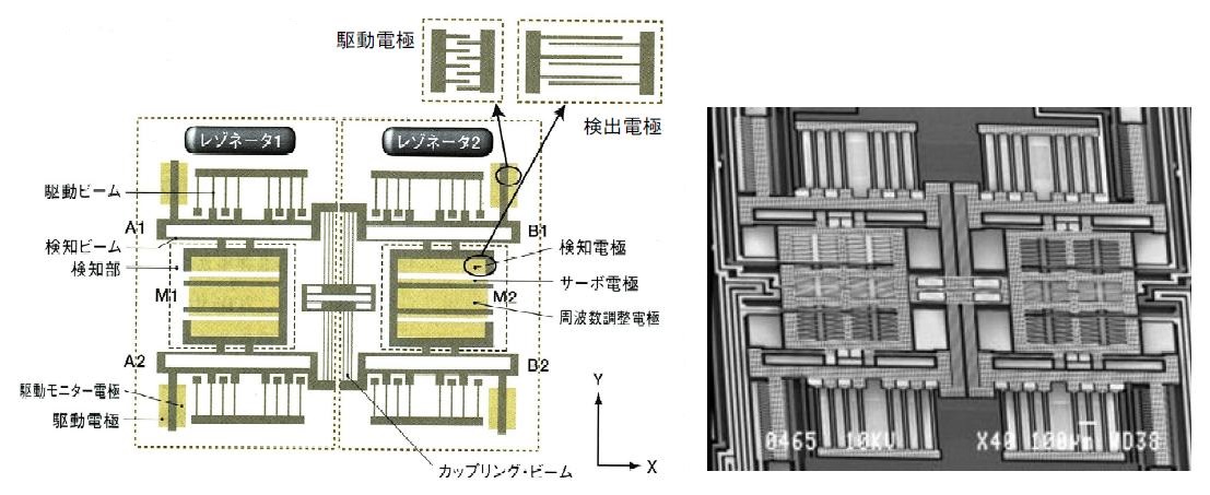 |
振動ジャイロ Vibration gyroscope
振動ジャイロは,おもりを一方向(x方向)に振動させておき,これが回転すると,コリオリ力によって直行方向(y方向)にも振動は発生する原理を用いた角速度センサです。トヨタ自動車は江刺教授らの研究成果をもとに上図の振動ジャイロを開発し,これはレクサスなどの車体安定化システム(Vehicle Stability Control System)に用いられています。A vibration gyroscope has an orthogonal 2-axis spring-mass system, where one axis is a driving axis and the other one is a sense axis. When the gyroscope rotates, vibration is excited by by Coriolis force in the sense axis. The vibration gyroscope shown in the above figure was developed by Toyota Motor based on research in Esashi Laboratory, and is used in a vehicle stability control system of LEXUS series etc.
 |
 |
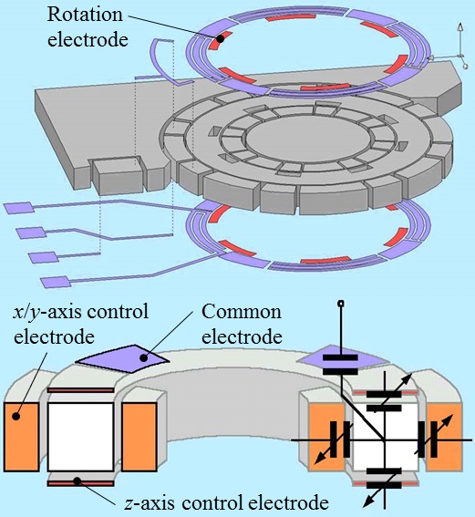
静電浮上回転ジャイロセンサ Electrostatically-levitated rotating gyro sensor
東京計器と共同で開発した静電浮上回転ジャイロセンサは,直径1 mmのシリコンリングを6軸デジタルフィードバック制御で静電浮上させ,約7万rpmで回転させることで,2軸の角速度と3軸の加速度を同時に計測します。これは,従来の振動ジャイロセンサと比べて桁違いに高い性能を有しており,地下鉄の乗り心地改善などに役立っています。また,歩行者ナビゲーション,ロボットの姿勢制御などへの応用も期待されています。An electrostatically-levitated rotating gyro sensor developed with Tokyo Keiki senses 2-axis angular velocity and 3-axis acceleration simultaneously. In the sensor, a silicon ring of 1 mm diameter is electrostatically levitated by 6-axis digital feedback control and rotated at about 70000 rpm. It has better performance compared with conventional vibration gyroscopes, and is used for the track maintenance of subways etc. The future applications include personal navigation and robot attitute control.
 |
 |
熱駆動型高周波MEMSスイッチの構造 |
高周波MEMSスイッチ(アドバンテスト) |
高周波MEMSスイッチ RF MEMS switch
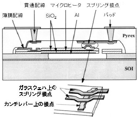
MEMSスイッチは機械的に接点をON/OFFする超小形スイッチです。このようなスイッチでは,接点が汚染されたり酸化されたりしないように,内部を清浄な環境に気密封止することが重要です。我々は,貫通配線付きガラスウェハの陽極接合によって気密封止された高周波MEMSスイッチを開発し,アドバンテストはこれをLSIテスタ用に実用化しました。この高周波MEMSスイッチは仙台の同社工場で生産され,地域の産業振興・雇用創出にも貢献しています。A MEMS switch has a metal-metal contact, which is mechanically turned on and off. For this type of switch, it is important to hermetically seal the contact in a clean environment to avoid the contamination and oxidation of the contact. Our key technology used here is wafer-level hermetic sealing by anodic bonding using a feedthrough glass wafer. The RF MEMS switch was commercialized by Advantest for LSI testers, and manufactured in their Sendai factory, contributing for the promotion of local industry.
 |
陽極接合できるLTCC基板 Anodically-bondable LTCC wafer
絶対圧センサ,加速度センサ,ジャイロ,MEMSスイッチなどの多くのMEMSは気密封止されています。我々は,ニッコーと共同でMEMSの気密封止に用いる陽極接合可能なLTCC(Low Temperature Cofired Ceramic)基板「Via-Wafer」を開発しました。従来からある積層セラミック基板の製造工程で,貫通配線はもちろん,内部配線や受動素子をLTCC基板内に作製できます。このLTCC基板による真空封止の高い信頼性は実証済みであり,MEMSの真空封止法の切り札として応用が広がっています(リンク 1,リンク 2)。Many MEMS including absolute pressure sensor, accelerometer, gyroscope and MEMS switch are hermetically packaged. We developed an anodically-bondable LTCC (Low Temperature Cofired Ceramic) wafer, "Via-Wafer", with Nikko for the wafer-level hermetic packaging of MEMS. Internal wiring and passive components as well as feedthrough can be fabricated in the LTCC wafer by the standard manufacturing process of laminated ceramic circuit boards. The LTCC wafer ensures hermetic sealing with high reliability and is being applied to a variety of MEMS.
 |
 |
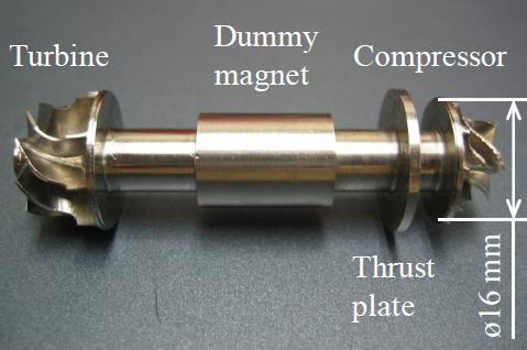
超小形ガスタービンのロータ(2007年) |
超小形ガスタービン発電機試作1号機(IHI,2012年) |
超小形ガスタービン発電機 Ultra-small gas turbine generator
2002年頃から自立ロボットなどのために超小形ガスタービン発電機を研究し,IHIなどと共同で,2007年,圧縮機翼車直径にして16 mmという世界最小のガスタービンエンジンのサイクル成立を達成しました(リンク)。2012年,IHIは上記成果を基に携行型超小形ガスタービン発電機の試作機を完成させました(リンク)。直径約8 cm×長さ12 cmの本体を含む全てのシステムがアタッシュケース内に納まっており,400 Wの定格発電出力を有します。既存のレシプロエンジン発電機と比べて静粛性や排気ガスのクリーン性に優れており,室内で使ってもストレスになりません。We started the development of an ultra-small gas turbine generator for robot application etc. around 2002, and demonstrated the operation of the world's smallest gas turbine engine, which has a compressor impeller of 16 mm in diameter, with IHI and other collaborators in 2007. In 2012, IHI prototyped a portable gas turbine generator based on our research. The system including an engine of 8 cm in diameter and 12 cm in length is installed in an attaché case, and has a rated electric power of 400 W. It is advantagous in quietness and the cleanness of emission compared with conventional reciprocating engines, and thus applicable to indoor use.
 |
 |
BST薄膜のレーザー支援トランスファによる可変SAWフィルタの作製法 |
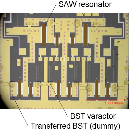
ワンチップ可変SAWフィルタ |
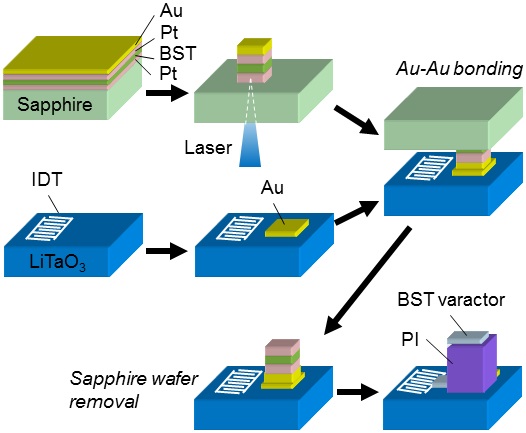
可変SAWフィルタ Tunable SAW filter
FIRSTプログラム(2010-2013年度)において,村田製作所,情報通信研究機構(NICT),および千葉大学と共同で,デジタルテレビジョン放送の空き周波数帯域(TVホワイトスペース)を選んで無線通信するためのワンチップ可変表面弾性波(Surface Acoustic Wave,SAW)フィルタを世界で初めて開発し,TVホワイトスペース対応のコグニティブ無線機に搭載して,通信デモンストレーションに成功しました(動画,リンク)。SAWフィルタに・戟[ザー支援トランスファ技術によって薄膜BST可変容量が集積化されており,薄膜可変容量の静電容量を変化させると,SAWフィルタのバンドパス特性が変化します。TVホワイトスペースの利用にあたっては,空き周波数帯域を選択するためのフィルタの小形化が課題でしたが,今回開発したワンチップ可変SAWフィルタは,TVホワイトスペースを利用するコグニティブ無線を携帯電話やスマートフォンなどで利用することに道をひらきます。We developed a monolithic tunable SAW (Surface Acoustic Wave) filter, which is used for cognitive radio communication using vacant digital TV channels, i.e. TV white space, with Murata Manufacturing, National Institute of Information and Communications Technology (NICT) and Chiba University in FIRST Program (FY2010-2013). The tunable SAW filter was installed in a cognitive radio system and worked successfully. Thin film BST varactors are integrated with the SAW filter by laser-assisted transfer technology, and the bandpass characteristic is tuned by the varactors. The developed tunable SAW filter opens the application of TV white space cognitive radio to mobile phones and smartphones, where the miniaturization of channel selection filters is a problem.
 |
 |
全真空ウェハ接合装置 |
原子層堆積装置 |
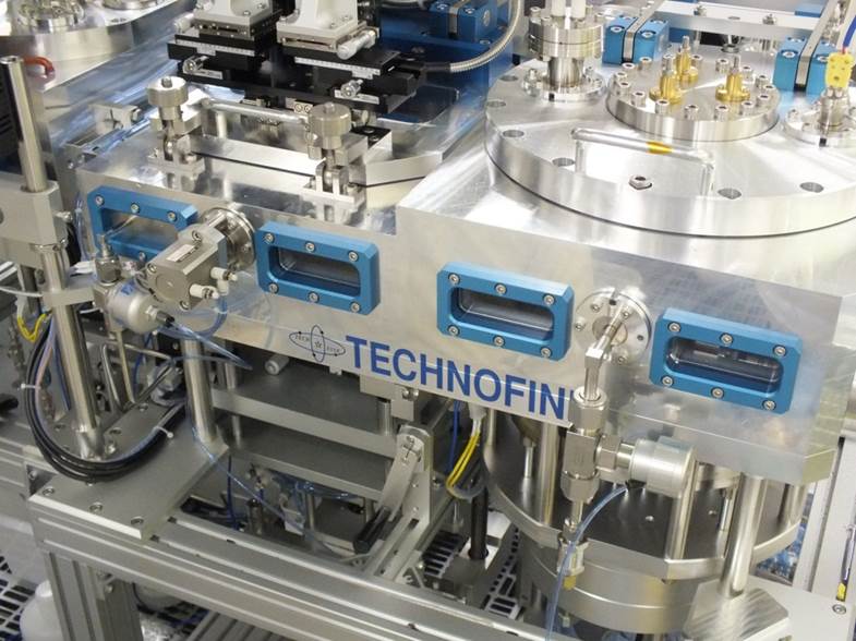
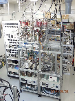
全真空ウェハ接合装置,原子層堆積装置 Through-vacuum wafer bonder and ALD system
先端融合イノベーション創出拠点の形成プログラム(2007-2016年度)において,ウェハの前処理,アライメント,接合,および冷却を一貫して真空中で行えるウェハ接合装置を開発し,集積化デバイスの試作,およびウェハレベルパッケージング技術や異要素集積化・Z術の開発に利用しています。また,昇華性原料と液体原料の両方を利用できる原子層堆積(Atomic Layer Deposition,ALD)装置を開発し,MEMSの試作に利用しています。この装置は,1台で複数種類の機能性酸化物と金属を複雑な3次元マイクロ構造に均一に成膜できます。これらの装置はテクノファインから市販されています(ウェハ接合装置・ALD装置・ホットワイヤ装置のパンフレット)。In Creation of Innovation Centers for Advanced Interdisciplinary Research Areas Program (FY2007-2016), we developed the wafer bonder where pre-treatment, alignment, bonding and cooling were sequentially done in vacuum. It is used for the fabrication of integrated microsystems and the development of wafer-level packaging and hetero-integration technology. We also developed the ALD (Atomic Layer Deposition) system which used solid and liquid sources. This ALD system can deposit multiple kinds of oxides and metals conformally on complicated 3-dimensional microstructures. These tools are commercially available from Technofine (Brochure of ALD system).