
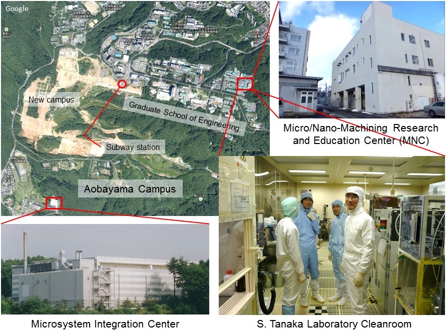
S. Tanaka Laboratory is using the following well-equipped facilities to develop MEMS. All members are allowed to access all of the facilities after a safety class. We are also taking care of many tools in the facilities.
Aobayama Campus from Drone (2017)
 Division of Mechanical Engineering
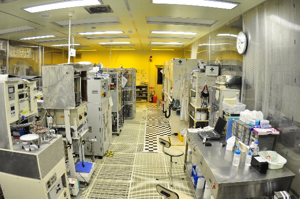 ・Cleanroom operated by S. Tanaka Laboratory
- 130 m2 nice cleanroom mainly for 20 mm substrates
- Many laboratory-made tools installed
- The best MEMS research environment for beginners to experts
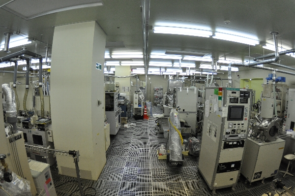 ・Micro/Nano-Machining Research and Education Center (MNC) [Link]
[Movie]
・Micro/Nano-Machining Research and Education Center (MNC) [Link]
[Movie]- Common facility belonging to Graduate School of Engineering
- 600 m2 and 150 m2 well-equipped cleanrooms and 6 common laboratories
- Many MEMS tools operated by S. Tanaka Laboratoy
Junichi Nishizawa Memorial Research Center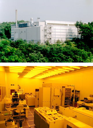 ・Jun-ichi Nishizawa Memorial Research Center
- Large common facility and rental spaces with 5000 m2 area in total
- Donation from Semiconductor Research Institute in 2008
・2F super cleanroom with 1800 m2 area [Movie]
- Open facility for MEMS development
- Many tools for 4 and 6 inch wafers
- Hands-on Access Laboratory system for spot users [Link]
・Project Laboratory in 3F cleanroom
・Administration office of Microsystem Integration Center (μSIC) [Link]
S. Tanaka Laboratory for Smart System Integration, Chair of Nanosystem, Department of Robotics, Tohoku University
Division of Mechanical Engineering, 6-6-01 Aramaki aza Aoba, Aoba-ku, Sendai, Miyagi 980-8579
TEL: 022-795-6937 FAX: 022-795-6935
Division of Mechanical Engineering, 6-6-01 Aramaki aza Aoba, Aoba-ku, Sendai, Miyagi 980-8579
TEL: 022-795-6937 FAX: 022-795-6935