
 Research and development of MEMS for various applications
MEMS (Micro Electro Mechanical Systems) are sensors and actuators based on semiconductor microfabrication technology, and widely used as pressure sensors, accelerometers, gyroscopes, microphones, bandpass filters, inkjet printer heads, projector image engines, infrared sensors/imagers. You may be using a smartphone, a tablet computer, a TV game machine and/or cars, in all of which MEMS are used as key devices. LSI (Large Scale Integrated Circuits) are the brains of machines, whereas MEMS are sensory systems and connect human and machines.
Our laboratory is globally recognized as one of the most active research groups in the field of MEMS and micro/nanotechnology. We have prototyped many devices such as pressure sensors, accelerometers, gyroscopes, acoustic wave filters, microvalves, the world's smallest gas turbine generator, micro fuel cells, RF MEMS switches, optical scanners, micro rocket thrusters, tactile sensors for robots and integrated biosensors. Also, we have developed key technologies such as wafer-level MEMS packaging technology, micro/nano fabrication technology and system integration technology. Some of these works have been commercialized by intensive collaboration with industry (Link).
Recently, MEMS are getting more important for advanced communication, automated control, healthcare, medical diagnosis, safety, energy saving etc. The global market of MEMS is continuously growing. Our recent research projects include CMOS integrated MEMS, MEMS with advanced functional materials, MEMS based on nanotechnology and new bio-microdevices. We believe that some of our outputs will be commercialized and make our daily life more healthy, comfortable and sustainable.
Brochure of S. Tanaka Laboratory (2024)
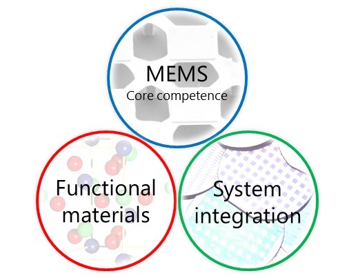 Fusion of heterogeneous core technologies |
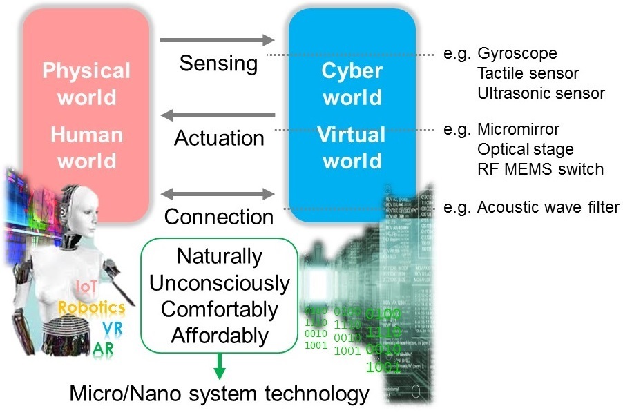 MEMS connecting human and machines |
Research topics- Sensor systems for human-friendly robots
- Integrated biosensors
- Frequency control devices for advanced wireless communication (SAW/BAW devices)
- Advanced inertial sensors for automated vehicles and robots
- Piezoelectric thin films and devices
- Heterointegration technology and wafer-level packaging technology
- Key technologies for sensors and microactuators
- MEMS process tools
To students who want to study MEMS and micro/nanotechnologyS. Tanaka Laboratory is aiming to create advanced device technologies, new ideas and concepts on future devices and systems, solutions to technological challenges in industry etc. Creating someting useful for human society and industry is our largest pleasure. Our core competence is MEMS technology.
We are very eager to collaborate with industry and working with a lot of companies. S. Tanaka Laboratory is in Department of Robotics, Graduate School of Engineering, to whichi all students are belonging, and also making project teams in Microsystem Integration Center (μSIC), which is organized for industrial collaborations. Our students are mainly in charge of academic researches which are investments for the future, but naturally learing practical engineeering in the environment where industrial collaborations are intensively ongoing. Our students have chances to collaborate with companies and to visit foreign research institutes and universities (Experiences from Student Blog).
We are developing not only devices but also systems, tools and materials. "Making various things by ourselves" is our motto, which differentiates us from many other laboratories. To realize our motto, we have well-equipped facilities and junior to senior members with various backgrounds. Furthermore, we are making a lot of efforts to make our laboratory internatinal (Voice of T. Bartley: JST website, Original) by accepting members from various countries and collaborating with foreign research institutes and universities. Our students who have learned a lot of skills in one of the world's best research environments are strongly requested by industry and academic fields.
If you are interested in MEMS, micro/nanotechnology or their applications, please join S. Tanaka Laboratory in Department of Robotics, Division of Mechanical Engineering. If you like making someting new, you need not have MEMS specialty, and on the contrary, your current specialty different from ours should be often helpful. Please do not hesitate to make a contact with us by e-mail.
Voices of our students from Student Blog: About research (English, Japanese) About internationality (English, Japanese)
Universities from which our members joined:
Tsinghua University, Zhejiang University, Harbin Institute of Technology, Politecnico di Torino, INSA de Lyon, Huazhong University of Science and Technology, University of Electronic Science and Technology of China, Technische Universität Chemnitz, Universidade Federal de Minas Gerais, Indian Institute of Technology Kharagpur, Hanoi University of Science and Technology, National Research Tomsk Polytechnic University, Shandong University, Chongqing University, Jilin University, University of Chile, University of Engineering and Technology Lahore, Dalian University of Technology, Xi'an Jiaotong University, Beijing Institute of Technology, Institut Teknologi Bandung, University of Science and Technology of China, University of Electronic Science and Technology of China, Universidad San Carlos de Guatemala, PSG College of Technology, Coimbatore etc.
Companies and universities which our international members entered:
Carnegie Mellon University, GLOBALFOUNDRIES, Sony, Southern University of Science and Technology, Mazda Motor, Huawei Technologies, MegaChips, Stanley Electric, Hitachi, TDK, Hiroshima City University, Tohoku University, Richo, AAC Technologies, Shanghai University, Toshiba, Institut Teknologi Bandung etc.
Admission routes
There are two routes of admission to S. Tanaka Laboratory:
(1) International Mechanical and Aerospace Engineering Course (IMAC-G)
(2) Regular Master's and Doctoral Degree Program
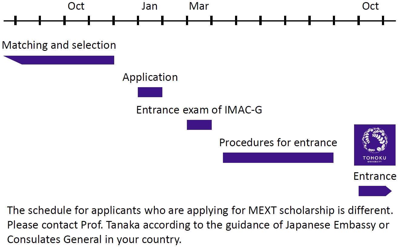
S. Tanaka Laboratory basically accepts international students via the first route (IMAC-G). For October 2022 enrollment, the application is in January 2021 and the entrance examination is in March 2021. The entrance examination is basically online.
Scholarship
MEXT scholarship: Please contact the Japanese Embassy or Consulates General in your country.
MEXT scholarship via university recommendation: Excellent students from the universities which have academic exchange with our university have the chance of application. Please contact us.
Internal full scholarship: Master course students who decided to proceed to the doctoral course have the chance of application.
Aobayama Campus from Drone (2017)
Tohoku University Promotional Video (2014)
Why don't you join us?
To industrial customers looking for a MEMS R&D partnerS. Tanaka Laboratory, belonging to Graduate School of Engineering and Microsystem Integration Center, is willing to support MEMS industry in research and development based on a lot of technology, know-how and literature accumulated for a long time from the previous laboratory, i.e. Esashi Laboratory. We can propose multiple styles of research and development, from the proof of concept using small substrates to device prototyping using 4-6 inch wafers, depending on R&D phase in each company. The proof of concept is conducted at the minimum cost and risk mainly using our cleanroom and Micro/Nano-Machining Research and Education Center (MNC). We accept researchers from companies, and they can experience the total process of MEMS development to be experts and key persons in their company's MEMS team. The visiting researcher has a chance to pursue his Ph.D as a graduate student. Prototype devices on 4-6 inch wafers are fabricated mainly in Microsystem Integration Center (Jun-ichi Nishizawa Memorial Research Center). Devices fabricated in our facilities can be commercially used with some reservations. Tools in Microsystem Integration Center can be simply used by visitors based on pay-by-the-hour system ("Hands-on Access Laboratory" system), but we recommend you collaboration with us not to lose time and money in a complacent manner, especially if you are not a MEMS expert. S. Tanaka Laboratory has a lot of experiences about difficult-to-access technologies such as wafer-level packaging, heterogeneous integration and piezoelectric thin films (Link 1, Link 2). Consultation about MEMS technology and business are being accepted anytime from companies. You can access us by e-mail.
Brochure of S. Tanaka Laboratory (2024)
[Home]
S. Tanaka Laboratory for Smart System Integration, Chair of Nanosystem, Department of Robotics, Tohoku University
Division of Mechanical Engineering, 6-6-01 Aramaki aza Aoba, Aoba-ku, Sendai, Miyagi 980-8579
TEL: 022-795-6937 FAX: 022-795-6935
Division of Mechanical Engineering, 6-6-01 Aramaki aza Aoba, Aoba-ku, Sendai, Miyagi 980-8579
TEL: 022-795-6937 FAX: 022-795-6935